


BrickTronic
-
Posts
110 -
Joined
-
Last visited
Content Type
Profiles
Forums
Gallery
Everything posted by BrickTronic
-
Hello, Assumptions are : Inactive : both lines low shift in "1" : Set upper Line from "0" to "1" and then back to "0" while lower Line remain "0" shift in "0" : Set lower Line from "0" to "1" and then back to "0" while upper Line remain "0" Strobe : at last Bit set upper or lower Line from "0" to "1" while lower upper is still "0" but then set the 2nd Line also to "1" At end of sequence set both Lines back to "0" The CLK of the Shift-Register is delayed by the OR-Gate. so that Data-In of Shift will be stable If necessary 2nd OR/AND Gate (with 2nd Pin wired to GND or VCC) secures sufficient propagation Delay If you use 74LS595 or CD4094, then the OR is wired to Shift-Clock and the AND to the Strobe-Clock When using 74LS164 with 74LS273 then the OR clocks the 164 and the AND the LS273 Both circuits can handle 8-Bit, in drawing I was lazy and draw only first 3 Bit Jo
-
Hello, A possible improvement to generate a Strobe out of Clock & Data Signals : A puls on upper Line shifts in a "1", a puls on lower Line shifts in a "0" and at last puls also 2.nd Line set to "H" issue a Strobe No need of additional Strobe-Line or to add 7th and 8th Puls to be use d as Strobe and Reset Jo

-
Hello, 74LS164 sounds much better But during shifting the Outputs does "flicker" but for Motors (or bulp-lamps) this might not be visible can also be avoided when adding an Latch like 74LS273 between Shifter-Output Bits and Output Connector to strobe the Data-bits I doubt you will answer to wire Ser-In to D_0-Parallel-Load of 74LS168 and wire all other D_n (n=1 to 7) parallel Load to Out_n-1 ... and use parallel Load feature of Counter for shifting :-) There are many roads to Rome or should I say ROM ;-) Jo
-
Hello, 74LS168 is an Up/Down Couter with Parallel Load. How does you shift in serial "random" Data using this Chip ? I would expect something like CD4094. By separate Strobe-Pin you can avoid "flikering" of Outputs during Shift activity. The CD4094 should also be usable for an Shart PC401 Interface Jo
-
Lego Smart Brick General Discussion/Concerns Topic
BrickTronic replied to a_clay_brick's topic in General LEGO Discussion
Hello, Excellent summary ! Can you share the Links that was shown on last slides ? Jo -
Hello, Thanks ! Looks very interesting. Can't wait to get more Info. Especially how USB-C Power Balancing is working and why there are the 4 "Magnetic"-Contacts used. Jo
-
Hello, @michaelgale There are 4 Contacts on each side of the Speed-Controller. For Power-Supply I expect only 2. Why are there 4 ? For what are the 2 additional used ? What happens when you connect 2 Speed-controllers antiparallel side-by-side ? Shortage ? When you have to use more USB-C injections for Power-Supply, how is secured Power-Balancing beteen them ? Is there Isolation-Tape between the two Supply-Groups necessary ? Or can this Supply to other Modules be switched OFF (ev. by configuration via USB ?) ? What are the technical Data of the Speed-Controller ? Where to find them ? What Power does the Spee-Controller support ? I assume you did much test with various Motors, so how moch motors can be driven (at what conditions on mechanical Load to be moved) ? And what is then the impact on Rail-Lenght between multi-point supply ? Can 2 or more Speed-Controllers work together for Multiple-Point-Supply (all outputs driven by a single Target-Value) ? Does the Speed-Controller support DCC ? Jo
-
Hello, (Where) Are the readouts of the TAGs available ? What Value does the TAG-Characters represent ? At which address in the TAG-Memory is the character-ID stored ? Jo Are there more RAW-Data than the 14 of the SmartPlay Tags known ? Bricklink reports 36 (Tiles + Figs)
-
Hello, Have a look at Brickcontroller2 Jo
-
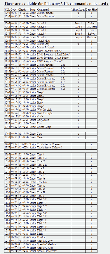
Hello, Reverse-Engineering of this Interface you can find on Youtube The Spybot uses not IR-Puls like RCX but a RS232--to-(visual)-Light Interface. There is Read and Write possible (4800Bd, 8-Data, Odd Parity, 1 Stop) VLL Output is above serial-Interface There is also a IR-Remote (76kHz 25% Duty) to can control the Spybot (same IR-Protocol as Bionicla-Mana, RC-Train and "Nitro-Flash") Unfortunately there is very less information available for Spybots (like available Memory-Size for Commands, used uC, Serial Protocoll and used Commands [possibly sub-set of RCX]) So if you want to extend supported PBricks (Programmable-Brick) please feel free ... By the way, the USB IR-Tower support IR for RCX & Co like also VLL Jo
-
Hello. I'm aware of (see png), Jo
-
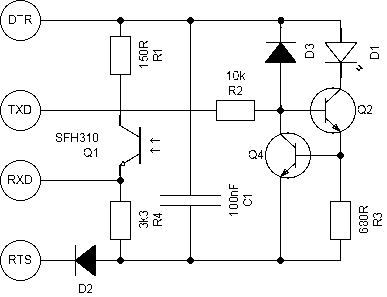
Hello Why not use same Methode used for Spybotic : And yes, you need also an TTL/RS232 Level-Translator like the good old MAX232 or compatible .. Jo
-
Hello, brown-red-red 12 00 -> 1k2 100% identified Thanks, Jo
-
Hello, C5 ? Maybe you mean C8, that in above schematic changed to C1 You wrote also 1k2, but in above Schematic R2 is now 2k2 2k2 would be color-code red-red-red or red-red-black-brown. In Photo of assembled PCB Top-side beside the 2 TO92 Transisors there is no red-red encoded resistor. 1k2 would be brown-red-red (or brown-red-black-brown), but I could also not identify this resistor on Photo. Color identification by photo is difficult What value is correct (Resistor placed at middle Pin of TO92) ? Jo
-
Hello, Are you willing to share the schematic diagram ? What uC and what H-Bridge Driver is used ? Jo
-
Sorry, hurts me like measure current in Volt and Voltage in Ampere ... There is mix-up of label 2's- and 1's- complement 2's complement is used to get the negatve expression of a value when working with negative / signed values (a Byte in range from 127 to 0 to -128) : 2's complement is : 256 - x (when x >0) for Bytes when x = 1 (0x01) then 2's complement of x result in 255 (0xFF) and stand for "-1" when you decrement n = 0x00 you get 0xFF so decrement (is n - 1) result in 0xFF alias -1 The 1's complement is just inverting each Bit of a Byte So 0x01 (binary 0000.0001b) becomes 0xFE (binary 1111.1110b) This is same as 255 - x (for x = 1) resulting in 254 (0xFE) or 0x00 becomes 0xFF And exactly this is used in RCX Messages Jo
-
Hello, Does you have taken pictures of you try to disassembling ? Would be great if you could share. Maybe not only me is interested. On Pybricks-Support Discussion there is not documented how Motor(s) can/will act as Broadcaster/Sender/Advertiser (of IMU-Data & Motor-Position/Speed) Is your code somewhere available ? A Link would be great. Jo
-
Hello, Did you also send unlock after power-up and periodic "Alive" ? And does you Toggle Command when sent miltiple time in sequence ? 3 9 13 17 23 29 34 39 45 51 57 62 68 74 80 86 92 98 104 109 115 120 126 132 138 144 150 156 162 167 173 178 184 190 196 202 208 214 220 226 232 237 243 248 254 259 265 271 277 283 289 295 301 306 312 318 324 329 335 341 347 0xFE 0x00 0x00 0xFF 0xA5 0x5A 0x44 0xBB 0x6F 0x90 0x20 0xDF 0x79 0x86 0x6F 0x90 0x75 0x8A 0x20 0xDF 0x62 0x9D 0x79 0x86 0x74 0x8B 0x65 0x9A 0x2C 0xD3 0x20 0xDF 0x77 0x88 0x68 0x97 0x65 0x9A 0x6E 0x91 0x20 0xDF 0x49 0xB6 0x20 0xDF 0x6B 0x94 0x6E 0x91 0x6F 0x90 0x63 0x9C 0x6B 0x94 0x3F 0xC0 0x85 0x7A #NV D o y o u b y t e , w h e n I k n o c k ? 3 9 14 20 25 31 37 43 49 55 61 67 72 78 83 89 94 100 105 111 117 123 129 135 140 146 152 158 164 170 176 182 187 193 199 205 211 217 223 229 234 240 245 251 257 263 269 275 280 286 292 298 303 309 315 320 326 331 337 342 348 354 360 365 371 376 382 388 393 399 404 0xFF 0x5A 0xA5 0x4A 0xB5 0x75 0x8A 0x73 0x8C 0x74 0x8B 0x20 0xDF 0x61 0x9E 0x20 0xDF 0x62 0x9D 0x69 0x96 0x74 0x8B 0x20 0xDF 0x6F 0x90 0x66 0x99 0x66 0x99 0x20 0xDF 0x74 0x8B 0x68 0x97 0x65 0x9A 0x20 0xDF 0x62 0x9D 0x6C 0x93 0x6F 0x90 0x63 0x9C 0x6B 0x94 0x21 0xDE 0xE8 0x17 0xFF 0x46 0xB9 0x46 0xB9 0xFF 0xEF 0x10 0xEF 0x10 0xFF 0xB5 0x4A 0xB5 0x4A #NV J u s t a b i t o f f t h e b l o c k ! 177 Set power down delay (minutes) 231 Alive 66 Set sensor mode (sensor, code) where code=mode,slope Documentation on available Opcodes are in the SDK Package available at Philo's Page (it is a selfextracting EXE-File) Inside this Zip-Container there is File RCX2 LASM byte codes.pdf in Folder .\L EGOMindstormsSDK25.exe\\program files\LEGO\LEGO Mindstorms SDK\Doc\ Without Unlock Sequence after Cybermaster Power-On no communicatiion passible. when Alive not received periodically, loss of communication (Time-Out -> Watch-Dog) Jo
-
Dacta Control Lab Software
BrickTronic replied to Dazmundo's topic in LEGO Technic, Mindstorms, Model Team and Scale Modeling
Hello, Maybe the Info in this thread might help (Page 3) : Jo -
Hello, Cybermaster us an "Tower" with RS232 Interface to PC and 27MHz Radio Frequency Interface to Cybermaster Pictures of the Tower : http://www.brickshelf.com/cgi-bin/gallery.cgi?i=604134 & http://www.brickshelf.com/cgi-bin/gallery.cgi?i=604133 and further http://www.brickshelf.com/cgi-bin/gallery.php?f=66485 Schematic you can find https://fccid.io/document.php?id=23750 Note that RTS = -12V and DTR=+12V is used for GND -> 5V to RS232 Level shift Programmable Prick Baudrate 0-Bit 1-Bit RCX 1.0 / 1.5 RCX 2.0 2.400Bd, Start- 8 Data-, Odd Parity- & Stop- Bit 4.800Bd, Start- 8 Data-, Odd Parity- & Stop- Bit 38kHz / 50% 76kHz / 25% Light OFF Light OFF Scout 2.400Bd, Start- 8 Data-, Odd Parity- & Stop- Bit 38kHz / 50% Light OFF Spybotic 4.800Bd, Start- 8 Data-, Odd Parity- & Stop- Bit Light ON Light OFF Cybermaster 2.400Bd, Start- 8 Data-, Odd Parity- & Stop- Bit AM 26,995MHz Programmable Prick Header Remark RCX 3 Byte 0x55 0xFF 0x00 Scout 3 Byte 0x55 0xFF 0x00 Spybotic tbd tbd Cybermaster 4 Byte 0xFE 0x00 0x00 0xFF Command to Cybermaster 1 Byte 0xFF Reply from Cybermaster Programmable Prick Command Frame RCX 0x55 0xFF 0x00 Cmd Cmd D0 D0 .. Dn Dn Chk Chk Scout 0x55 0xFF 0x00 Cmd Cmd D0 D0 .. Dn Dn Chk Chk Spybotic tbd Cybermaster 0xFE 0x00 0x00 0xFF Cmd Cmd D0 D0 .. Dn Dn Chk Chk Programmable Prick Reply Frame RCX 0x55 0xFF 0x00 Cmd Cmd D0 D0 .. Dn Dn Chk Chk Scout 0x55 0xFF 0x00 Cmd Cmd D0 D0 .. Dn Dn Chk Chk Spybotic tbd Cybermaster 0xFF Cmd Cmd D0 D0 .. Dn Dn Chk Chk Jo
-
Dacta Control Lab Software
BrickTronic replied to Dazmundo's topic in LEGO Technic, Mindstorms, Model Team and Scale Modeling
12V ??? The Interface A operates with 4,5V (Motors & Lights) The Opto-isolates parallel Inteface is using 5V from "Host" So an FTDI like Interface would work Jo -
Hello, very interesting document. With an G850VS you have luck to have an PIO Harware on the 11-Pin Port With an 1401 you can write Data (for example by LPRINT) to an external Interface to use them for Interface 9750 But the 2 Inputs might than be accessable only by Assembler-Code (or Peek/Poke Subroutine) ... Is there a schematic drawing of the GV850VS available ? wher can I find ? Or is there a Datasheet for the SC61680 Processor available ? how operates Xin/Xout there (especially the 2kHz/4kHz Mode and how to read Xin frequency) Johannes
-
Lego Smart Brick General Discussion/Concerns Topic
BrickTronic replied to a_clay_brick's topic in General LEGO Discussion
Hello, Maybe this https://www.dajlab.org/jtoypad.html might work ... Also have a look especially here https://www.dajlab.org/jcontrollab.html Unfortunately the WEDO 1 Hub is not supported on this page https://www.dajlab.org/index.html Jo -
Hello, Yes, will work, depending on Switch S1 Position an Address in Range 0x390 to 0x39F You also can remove R2 and wire IC6 (I think there is no IC6b ) Pin 3 direct to 5V ... Hope you will report success soon and how your "Hack" looks like Jo
-
Hello, The good old Wired-OR will work. You mentioned that it would be easier to use a 74LS138. Then only wire the Diodes-Kathode to Switch and all Anodes together with Pull-Up-Resistor (Wired-AND). This Diode-Point inverted (you can re-use IC3a or IC3b) with output to IC1a NAND-Gate But why not use 74LS85 to compare A0 to A2 to a 3-Bit DIP-Switch ? Anyhow, there are many ways ro ROMe :-) Have fun and let us participate how it is working ! Jo